Introduction
As semiconductor manufacturing pushes the boundaries of miniaturization, traditional water purification methods struggle to keep pace. Our breakthrough ultrafiltration technology redefines what's possible in ultra-pure water (UPW) production, delivering unprecedented purity levels essential for cutting-edge chip fabrication. With proprietary membrane science and precision manufacturing, we provide semiconductor fabs with a critical competitive advantage in water treatment.
")
Unmatched Performance for Advanced Nodes
1. Absolute Particle Control
• Engineered to remove 100% of particles >0.025μm
• Specialized surface charge modification prevents nanoparticle adhesion
• Verified performance at <1 particle/mL (>0.05μm) in final UPW
2. Ultimate Biological Security
• Antimicrobial membrane matrix inhibits microbial growth
• Validated endotoxin removal to <0.05 EU/mL
• Integrated biofilm prevention technology
3. Chemical Purity Assurance
• Ultra-low extractables (<0.1ppb TOC contribution)
• Certified for use in high-oxidation potential environments
• Resistant to all common CIP chemicals
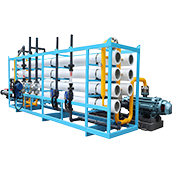
Cutting-Edge Membrane Technology
Our patented TriMatrix™ membrane architecture combines three distinct filtration mechanisms:
1. Molecular Sieving Layer
Precisely engineered pore structure
Uniform 0.01μm pore size distribution
Absolute particle retention
2. Electrokinetic Barrier
Zeta potential control for charged species
Enhanced removal of ionic contaminants
Reduced fouling potential
3. Hydrophilic Separation Matrix
Water flux optimization
Organic fouling resistance
Exceptional cleanability
")
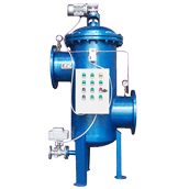
Smart Filtration Systems for Industry 4.0
Our intelligent UF platforms incorporate:
1. Real-Time Performance Monitoring
• Integrated particle counters
• TOC and conductivity sensors
• Predictive fouling analytics
2. Automated Optimization
• AI-driven cleaning cycle adjustment
• Self-adjusting flux management
• Remote performance diagnostics
3. Seamless Integration
• Industry-standard communication protocols
• Plug-and-play UPW system compatibility
• Scalable from pilot to full production
Application-Specific Solutions
1. EUV Lithography Water Systems
• Special low-metal elution construction
• Certified for <0.01ppt metal contamination
• Radiation-resistant materials
2. 3D NAND Fabrication
• High-capacity stacking configuration
• Optimized for organic removal
• Low-pressure operation
3. Advanced Packaging
• Compact modular designs
• Rapid flush capability
• High recovery operation
Verified Results in Leading Fabs
1. Our technology has been adopted by multiple top-tier semiconductor manufacturers, demonstrating:
• 70% reduction in water-related defects
• 45% decrease in chemical consumption
• 99.9% uptime reliability
• Consistent compliance with SEMI F85 standards
2. One recent implementation at a 5nm logic fab achieved:
• UPW resistivity >18.24 MΩ-cm continuously
• Particle counts below detection limits
• Zero unplanned maintenance events in first year
")
The Economic Advantage
Our solutions deliver substantial financial benefits:
• 40% lower capital expenditure vs traditional systems
• 30% reduced operating costs
• 60% longer membrane lifespan
• Fast ROI typically <12 months
Partnering for Success
We offer comprehensive support:
• Process water audits
• System design services
• Installation supervision
• Ongoing performance optimization
Discover how our revolutionary ultrafiltration technology can transform your semiconductor water treatment. Contact our experts today for a customized solution evaluation.
Q&A
Q: What's the typical water recovery rate?
A: 85-95% recovery rate in most applications.
Q: Can UF remove endotoxins?
A: Yes, effectively removes endotoxins from water.
Q: How often should membranes be replaced?
A: Typically every 3-5 years with proper maintenance.