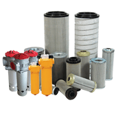
Introduction
In today's semiconductor industry, where process nodes continue shrinking below 5nm, water quality requirements have become more stringent than ever. Conventional filtration methods can no longer guarantee the ultrapure water (UPW) standards needed for advanced wafer fabrication. Our cutting-edge ultrafiltration (UF) membrane technology provides semiconductor manufacturers with an advanced pretreatment solution that consistently delivers water purity meeting the most rigorous industry specifications.
As a specialized manufacturer with complete vertical integration, we've developed proprietary UF membrane formulations specifically optimized for semiconductor applications. Our production process incorporates military-grade quality control measures to ensure every membrane module meets exacting performance standards while maintaining competitive pricing through efficient manufacturing.
Critical Performance Advantages for Semiconductor Water Systems
1. Unparalleled Particle Removal Efficiency
• Achieves >99.99% removal of particles down to 0.03μm
• Effectively eliminates colloidal silica that can damage sensitive processes
• Maintains consistent performance even with fluctuating feed water quality
2. Advanced Bio-Contamination Control
• Special surface modification inhibits bacterial adhesion
• Reduces endotoxin levels to <0.1 EU/mL
• Minimizes biofilm formation risk in distribution systems
3. Chemical Resistance for Harsh Environments
• Withstands extreme pH cleaning cycles (pH 1-13)
• Resists oxidation from ozone and peroxide treatments
• Maintains integrity when exposed to organic solvents
")
Technical Superiority Through Material Innovation
Our research team has developed next-generation membrane materials that outperform conventional UF technologies:
1. Nano-Enhanced Composite Membranes
Incorporates inorganic nanoparticles for enhanced mechanical strength
Provides superior chemical stability compared to standard polymers
Enables higher operating pressures without fiber breakage
2. Asymmetric Pore Structure Design
Gradient density structure prevents deep particle penetration
Allows more efficient backwashing with lower energy consumption
Extends membrane service life by reducing irreversible fouling
3. Antistatic Surface Treatment
Prevents particle adhesion through electrostatic repulsion
Particularly effective for silica and other charged contaminants
Reduces cleaning frequency by up to 40%
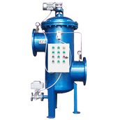
Customized Solutions for Diverse UPW Applications
Understanding that different semiconductor processes have unique water requirements, we offer tailored configurations:
1. Front-End-Of-Line (FEOL) Modules
• Ultra-tight pore structure for critical cleaning steps
• Certified metal ion levels below 1ppt detection limits
• Special low-extractable material construction
2. Back-End-Of-Line (BEOL) Solutions
• Optimized for organic contaminant removal
• Compatible with copper/low-k dielectric processes
• Integrated particle monitoring ports available
3. Photolithography-Grade Systems
• Exceptionally low TOC contribution (<0.3ppb)
• Bubble-point tested for absolute integrity
• Gamma-sterilizable versions for sensitive applications
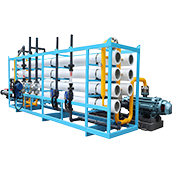
Implementation Case: 300mm Fab UPW System Upgrade
A Tier 1 foundry recently implemented our UF technology in their latest 300mm facility, achieving:
• 60% reduction in particle-related wafer defects
• 35% decrease in DI water consumption
• 50% extension of RO membrane replacement intervals
• UPW quality consistently meeting SEMI F78 specifications
The system demonstrated remarkable stability through 18 months of continuous operation, with no measurable performance degradation.
Why Semiconductor Manufacturers Choose Our Technology
1. Uncompromising Quality Assurance
• Every membrane lot undergoes full characterization testing
• Cleanroom assembly prevents particulate contamination
• Full material traceability with batch-specific documentation
2. Rapid Deployment Capability
• Standard modules available from regional stock
• Custom systems delivered in as little as 4 weeks
• Global technical support network
3. Total Cost of Ownership Advantages
• 20-30% lower lifetime costs versus competitors
• Energy-efficient operation reduces utility expenses
• Simplified maintenance reduces labor requirements
")
Future-Ready Ultrafiltration Solutions
As semiconductor technology advances toward 2nm nodes and beyond, we continue to innovate:
• Developing graphene-enhanced membranes for next-gen applications
• Implementing AI-driven performance monitoring systems
• Expanding our nanotechnology research program
Our commitment to semiconductor water treatment excellence ensures our partners always have access to the most advanced UF solutions available.
Contact our technical team today to discuss your specific UPW requirements and discover how our ultrafiltration technology can optimize your water treatment processes.
Q&A
Q: Is UF suitable for food processing?
A: Widely used in beverage, dairy and juice industries.
Q: How to calculate system capacity?
A: Membrane area × flux rate × operating hours = daily capacity.
Q: Can UF remove algae?
A: Yes, effectively filters out algae cells and blooms.