Reverse Osmosis Equipment for Semiconductor Ultra-Pure Water Production
Reverse osmosis equipment for semiconductor industry serves as primary purification unit to prepare ultra-pure water for wafer etching, cleaning and chip manufacturing. It is equipped with high-precision liquid filter as critical pretreatment barrier to intercept particulate pollutants and prevent irreversible RO membrane fouling. Users can adopt mature units such as Industrial-grade RO reverse osmosis system and 200 tons/hour large-scale reverse osmosis unit to build a complete semiconductor water treatment workflow. This system efficiently removes silica, heavy metals, soluble salts and colloids to reduce micro-defects on wafer surfaces and improve chip yield. Scalable configurations ranging from compact skids to large centralized RO units satisfy semiconductor fabs and integrated circuit industrial parks. Widely deployed in wafer fabrication, packaging and testing workshops, this article elaborates product composition, working principle, technical indicators, quality standards, application scenarios and typical operation challenges to support your semiconductor factory water treatment project planning.

1. Product Introduction
Reverse osmosis equipment for semiconductor industry is high-standard anti-fouling reverse osmosis system customized for ultra-pure water pretreatment in semiconductor manufacturing. In wafer fabrication, chip etching, photolithography and packaging processes, water purity directly determines product yield. Raw water contains silica, calcium-magnesium hardness, trace heavy metals, colloids and fine suspended particles. If these contaminants enter production links, they will form particle defects, metal contamination and oxide residues on wafer surfaces, leading to leakage, short circuit and performance degradation of finished chips. Therefore, stable reverse osmosis pretreatment equipment is an indispensable front-end facility of semiconductor ultra-pure water production line.
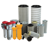
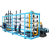
The whole equipment adopts heavy-duty modular skid-mounted design. All water-contact pipelines adopt high anti-corrosion materials to adapt to complex water quality environment. Front pretreatment system is equipped with high-performance liquid filter to intercept fine particles, colloids and precipitates, protecting downstream RO membrane elements from permanent fouling.
Enterprises can select specifications according to daily water consumption: small semiconductor pilot lines adopt reverse osmosis water treatment equipment (1+ ton/hour); medium-sized packaging factories choose Industrial-grade RO reverse osmosis system; large wafer fabs deploy multiple parallel sets to form 200 tons/hour large-scale reverse osmosis unit. For advanced process nodes requiring UPW, this RO host can be matched with two-stage RO and EDI to further reduce ion and particle concentration.
Many semiconductor process engineers distinguish this semiconductor dedicated RO equipment from ordinary industrial RO devices. Conventional reverse osmosis systems lack targeted high silica rejection design and strict particle interception capacity. Reverse osmosis equipment for semiconductor industry adopts high-rejection, low-fouling RO membranes with excellent silica removal performance. The permeate water after RO treatment serves as feed water for subsequent ion exchange or EDI ultra-pure water equipment. Separated concentrated water can be recycled for site cleaning after recovery treatment. Different from general water purification equipment, semiconductor RO system pursues stable ion rejection rate, low particle leakage and long-term continuous stable operation, and has become standard supporting equipment for newly built and upgraded semiconductor ultra-pure water stations.

2. Working Principle of Reverse Osmosis Equipment For Semiconductor Industry
Reverse osmosis adopts pressure-driven physical membrane separation technology. Under external driving pressure higher than raw water natural osmotic pressure, water molecules penetrate semi-permeable high-rejection RO membranes. Silica, soluble salts, heavy metal ions, colloids and suspended particles are trapped on the concentrated water side, realizing deep raw water purification as pretreatment of semiconductor ultra-pure water.
The complete semiconductor factory water treatment workflow is divided into four core stages:
Stage1: Multi-stage precision pretreatment filtration
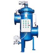
Raw water sequentially flows through multimedia filter, activated carbon filter and liquid filter. This process removes suspended solids, residual chlorine and large colloids, reduces turbidity and SDI value, and provides qualified inflow for RO main unit.
Stage2: Dosing regulation and pressurization
Special anti-scaling agent for silica and biocide are added quantitatively to restrain membrane scaling and microbial growth. Pretreated qualified water is boosted by anti-corrosion high-pressure pump to reach optimal operating pressure of semiconductor-grade RO membranes.
Stage3: Reverse osmosis deep purification separation
Pressurized raw water enters membrane pressure vessels. RO membranes intercept various pollutants, and water is divided into two streams: pre-purified permeate water for ultra-pure water system and high-salinity concentrated wastewater containing silica and heavy metals.
Stage4: Intelligent monitoring and automatic flushing
PLC control system continuously monitors conductivity, operating pressure and liquid tank level. Automatic cross-flow flushing activates during shutdown to wash colloids and precipitates attached on membrane surfaces. Operators can set periodic chemical cleaning cycles according to raw water silica content.
For advanced logic chip and memory production requiring ultra-high purity water, two-stage reverse osmosis configuration is strongly recommended.
3. Core Technical Parameters
We carry out personalized customized design based on semiconductor factory daily water output, raw water quality and ultra-pure water technical standards. Standard technical indicators of reverse osmosis equipment for semiconductor industry are as follows:
Water production capacity: 1m³/h ~ 200m³/h, customizable, covering reverse osmosis water treatment equipment (1+ ton/hour), industrial-grade RO reverse osmosis system and expandable 200 tons/hour large-scale reverse osmosis unit
Single-pass salt rejection rate: ≥98%, silica interception efficiency ≥93%
System water recovery rate: 60% ~ 75%, adjustable according to raw water silicon content
Outlet water conductivity: ≤5μS/cm, stable as feed water for follow-up UPW system
Inlet water requirements after pretreatment: Turbidity ≤0.1 NTU, SDI ≤3, residual chlorine <0.05mg/L
Working temperature: 5℃ ~ 40℃
Control mode: Full-automatic PLC intelligent control, online conductivity monitoring, high-low pressure protection, automatic membrane flushing, reserved timing chemical cleaning interface
Material specification: FRP / 316L stainless steel pressure vessel; anti-corrosion pipeline; semiconductor dedicated high silica rejection anti-fouling RO membrane
4. Product Quality Standard
All reverse osmosis equipment for semiconductor industry implements strict high-end electronic industrial water treatment equipment standards.
Firstly, core RO membrane elements adopt high-rejection anti-silica reverse osmosis membranes specially used for electronic industry. Supporting liquid filter uses high dirt-holding filter material to guarantee stable pretreatment effect and prevent particle scratch on membrane surface. High-pressure pumps, sensors and valves select anti-corrosion industrial brands suitable for long-term uninterrupted operation.
Secondly, every complete set of equipment passes hydraulic pressure test and 72-hour continuous running simulation test before delivery. The skid base adopts heavy-duty anti-rust anti-corrosion coating to adapt to clean workshop environment. We provide complete P&ID flow drawings, installation guidelines and operation manuals.
You can refer to the introduction of Industrial-grade RO reverse osmosis system for medium-scale semiconductor factory scheme reference.
Thirdly, our professional technical team provides remote online guidance and optional on-site commissioning service. Standardized maintenance plans effectively slow down silica scaling and organic fouling, extend membrane service life and ensure continuous stable water supply for wafer production lines.

5. Application Fields of Reverse Osmosis Equipment For Semiconductor Industry
This dedicated semiconductor reverse osmosis pretreatment system is widely used in integrated circuit manufacturing industry:
Wafer fabrication plant: Photolithography, etching, thin film process ultra-pure water pretreatment
Semiconductor packaging & testing workshop: Wafer cleaning, chip rinsing supporting pre-purified water
Display panel manufacturing factory: Array and cell process water pretreatment
Compound semiconductor production: Silicon carbide, gallium nitride wafer cleaning water preparation
Medium-sized electronic factory: Adopt industrial-grade RO reverse osmosis system
Large semiconductor industrial park: Deploy parallel 200 tons/hour large-scale reverse osmosis unit for centralized water treatment
Different process nodes of semiconductor manufacturing have differentiated strict requirements on silica, particles and metal ion content. Our engineers optimize pretreatment scheme and dosing parameters after analyzing local raw water samples, to match ultra-pure water technical specifications of chip production.
Frequently Asked Questions (6 Groups)
FAQ1
Q: Why cannot ordinary industrial RO equipment be used for semiconductor ultra-pure water pretreatment?
A: Ordinary RO equipment has limited silica interception capacity and poor particle blocking performance. Semiconductor-grade reverse osmosis equipment uses high-silica-rejection membrane materials, strict pretreatment matching and low-fouling design to avoid metal contamination and wafer micro-defects.
FAQ2
Q: How to select suitable reverse osmosis equipment model for semiconductor projects?
A: Small pilot production lines select reverse osmosis water treatment equipment (1+ ton/hour). Medium packaging factories choose Industrial-grade RO reverse osmosis system. Large wafer fabs can expand to 200 tons/hour large-scale reverse osmosis unit.
FAQ3
Q: What is the function of liquid filter in semiconductor RO water system?
A: Liquid filter intercepts fine suspended particles, colloids and precipitates in raw water, prevents hard particles from scratching RO membrane surface, reduces silica fouling risk and extends service life of high-performance semiconductor RO membrane elements.
FAQ4
Q: Can this reverse osmosis equipment run continuously matching 24-hour wafer production lines?
A: Yes. The whole system is optimized for non-stop industrial operation, equipped with automatic flushing and timing cleaning functions, adapting to uninterrupted continuous production rhythm of semiconductor factories.
FAQ5
Q: Is two-stage reverse osmosis necessary for all semiconductor projects?
A: Single-stage RO meets basic pre-purification requirements for packaging process. Two-stage reverse osmosis is recommended for advanced node wafer fabs and memory chip production requiring ultra-low ion and silica content.
FAQ6
Q: What regular maintenance tasks should be arranged for semiconductor RO equipment?
A: Regularly replace filter cartridges inside liquid filter; maintain stable dosage of anti-silica scale inhibitor; activate automatic membrane flushing; monitor inlet and outlet conductivity and silica index daily; carry out chemical cleaning once scaling leads to water yield decline.
Other products you want to know about:
RO membrane
High Flow Cartridge Filter
Ultrafiltration equipment